Exploring Machine Learning Applications in Wafer Characterization Technologies
Author: PRATUL VENKATESH
Title: Exploring Machine Learning Applications in Wafer Characterization Technologies
Published: 9 SEPTEMBER 2024
Originally written: 23 MARCH 2024
URL: https://www.pratulv.com/sci-tech/machine-learning-for-semiconductor-wafer-characterization
Email: pratulvenkatesh@outlook.com
Abstract
Advances in machine learning technologies have enabled their utilization across various processes in the semiconductor industry, where optimization is a persistent goal. The paper explores the applications of machine learning in wafer characterization technologies – an essential component in the chip development process – ranging from technologies such as profilometry, interferometry, ellipsometers, electron probe microscopes, atomic force microscopy, etc. It highlights the kind of problems that can benefit from a machine learning approach, analyses current limitation of wafer characterization technologies, current solutions being explored and other potential future applications, and in this ever increasingly data-driven world explores applications such as defect detection, tuning automation, fault diagnosis, increased measurement accuracies, and ability to perform non-destructive in-situ measurements. Overall machine learning algorithms can automate a lot of processes that are currently time consuming, laborious, wasteful, or requiring expert intervention.
Introduction
The semiconductor wafer and chip fabrication industry has always been driven by a demand for miniaturization, optimization and reducing costs, with driving motivations such as increased computation power, lower power consumption and efficient mass production to meet the ever-increasing demand for computer chips.
In the process of the wafer fabrication, reliable and accurate characterization technologies are an essential component across all stages of the fabrication process – across initial research and development stages all the way till mass production to ensure defect free production. Ideal characterization technologies are cheap, efficient, and able to perform non-destructive in-situ measurements.
Advances in machine learning (ML) algorithms and artificial intelligence have made them more feasible and available for a wide range of applications, helping achieve optimization and cost reduction goals in general across the industry. The key requirement for effectively utilizing these advances is the availability of large, clean, and labelled training datasets, though in instances without the availability of such data, unsupervised learning ML algorithms may also sometimes present effective solutions.
Wafer characterization technologies have limitations such as the efficiency, cost, limit of resolution, complex data analysis processes, wafer constraints, inability to perform non-destructive in-situ measurements, limit on kind of datatypes, ineffectiveness without large amounts of experimental datapoints, need for prior predictions of datapoints, etc. While all of these are not solvable directly with the help of machine learning, machine learning can help improve, optimize, or automate processes in some of the limitations and challenges mentioned.
The paper explores the scope and limitations, and the current and potential applications of machine learning algorithms in wafer characterization technologies specifically identifying the kinds of problems that machine learning algorithms can help solve, and which wafer characterization technologies can benefit from these ML algorithms.
When is a machine learning algorithm useful?
A ML algorithm is a smart algorithm that learns from training data to be able to perform a complex calculation task. Various kinds of ML algorithms exist such as neural networks- a series of mathematical formulations with nodes, layers, input biases and activation functions. These neural networks are inspired by the neural activity in our brain – with similar functionality to how certain pathways get stronger with more use (the learning aspect of ML.) ML algorithms can help achieve computation task where a machine can be taught to perform specific tasks – image classification, anomaly detection, prediction and forecasting, process automation, etc.
The key requirement for an ML algorithm is the prior collection of data that will form the training dataset. A large dataset with many examples of the kind calculation required to be performed, and a good balance of varied data points (in order to prevent overfitting or underfitting – a instance where the machine learning algorithm amplifies noise patterns or fails to identify the patterns, we need it to see.) Once trained the ML algorithm can perform the same computation task for any new sets of data, and overtime gets better and more tuned at performing this task.
To train and employ machine learning algorithms one needs cleaned datasets (no missing data points in different fields/columns, datapoints of a defined variable type across all records, etc.) with labelled outputs. Such an example could be the input gas flows parameters, environmental conditions – temperature, pressure, etc. – that go into a deposition process. In many instances in the semiconductor wafer fabrication process, mathematical formulations from derivations, solutions of partial differential equations, numerical methods, etc. can offer direct computational results however a machine learning algorithm can be a useful alternative when there are numerous input parameters to be considered with complex relationships and dynamic conditions that may change over time and vary significantly across processes, whose mathematical formulation and modelling otherwise is almost as is trying to predict chaos. Machine learning algorithms with multiple layers end up modelling polynomial equations (using approximations instead) through its layers.
In the instances where there is no labelled data on what the outputs are, machine learning algorithms can try and identify patterns and present possible outputs, that can then be interpreted and labelled as per the required process. Thus, machine learning algorithms provide a wide range of applications – where it is especially useful in handling multiple inputs with complex relationships and may be dynamically changing over time. It presents applications such as classification, categorization, anomaly detection, linear regression, predictions, etc. and with the introduction of feedback loops can also automatically update its parameters – learning new conditions, behaviors – which can be useful for automating processes and tasks by human operators.
What are the current limitations of wafer characterization technologies that could benefit from machine learning?
Wafer characterization technologies range across the following: atomic force microscopy, ellipsometry, scanning tunnelling microscopy, scanning electron microscopy, photoluminescent measurements, transmission electron microscopy, and secondary ion mass spectrometry. Each of these technologies have different strengths – in their efficiency, accuracy, resolution limits, types of data that they can measure, etc. and drawbacks – prohibitive costs, complex operations, destructive (wafer cannot be further used again) measurements, etc.
The need for destructive measurements could be reduced if a machine learning algorithm could be trained to detect anomalies (by considering previous experimental data encompassing internal and external process parameters such as environmental conditions) or be able to predict variables using non-destructive methods (for example defect detection with only a microscope image.) ML algorithms can be trained to remember any number of patterns, thus while a certain measurement may appear to be as noise to a human interpreter, a ML algorithm can predict even what the noisy measurements may be.
Certain characterization technologies such as ellipsometry require an estimate of the profile, and knowledge of the layers present to be able to create the formulation and fitted parameters. In instances where the layer profile may change due to anomalies or uncontrollable conditions, for example in thin film silicon nitride refractive index changes because of varying film density and quality due to varied gas flows inside the deposition chamber (because of leaks, built up pressure in bends, etc.) the measurement accuracy significantly drops.
Atomic Force Microscopy requires prior knowledge of the surface structure to choose the right probe for measurement – that can provide accurate results as the measured line width is dependent on the probe shape.

Fig. 1. Probe shape dependency of measured line width with true profile obtained from profiling standard samples and known probe tip shape (Ref. [1]).
In Scanning Tunnelling Microscopy, the tunnelling current measured in very weak and needs to be amplified. Weak signals are generally prone to high amounts of noise and distortion that may be difficult to accurately and reliable discern without having to significantly tune to the signal.
In many wafer characterization technologies, prior knowledge of the materials, material spectrums, etc. is required however quality and density variance can lead to minor changes and shifts in the spectrums, as some materials may have multiple bandgaps that may not always be activated, or film stress and strain may also induce bandgap shifting. Having to tune to such shifts every time a process changes slightly leads to prohibitive increase in costs – such as numerous experimental re-runs required or the requirement of more expensive equipment such as electron microprobes to re-measure material characteristic profiles.
What are the current applications of machine learning in wafer characterization technologies?
In the scale of mass production, it is economically unviable to manually inspect every chip for defects. A major application of machine learning currently being employed is towards pattern detection of defects on the wafer, where measurements through simple and faster profilometry or interferometry generated a wafer map that consists of images of defects and various types of wafers. Through the employment of pattern detection, a wafer can be pre-emptively screened [2] for any potential defects that are then finally measured and confirmed with the help of more accurate (but inefficient relative to the scale of mass production) forms of wafer characterization such as electron probe microscopy.
The requirement for the above implementation was the creation of large datasets with wafer maps and labelled data on the locations of defects present. The dataset was used to train the machine learning algorithm, where through image classification and computer vision algorithms can help predict current defects or imminent defects. [3] Imminent defects are predicted through failure clusters, where a concentrated region of dies that failed inspection can help analyse the cause of the defect, in a more timely and automated manner, thus significantly making mass production processes more efficient and able to help diagnose causes of defects considering that data for all processes are constantly being collected with not much active analysis being performed into the data (the data is usually checked only if a defect is detected.) [4]
Another application of machine learning currently being explored is the use of deep (many layer) neural networks to help automate the process of solving inverse ellipsometric problems in ellipsometers that have traditionally require human expert intervention and numerous trial and error processes to be able to get an accurate result. The trained machine learning algorithms were reliable even on a broad range of films materials across di-electrics, semiconductors doped and un-doped, and metals. Ellipsometry measurements employ the use of fitting techniques that rely on trial and error learning and require an initial estimate on the wafer characteristics. The machine learning algorithm considers transmission and reflection spectroscopies to help predict initial parameters – wafer film thickness, refractive index, in a closed loop feedback model. Thus, this can help automate the tuning and fitting process for minor variations in film thickness or refractive index, significantly making measurement processes more efficient and thus more accessible.
Machine learning algorithms have also been used to detect contaminated and blunted probes in the case of atomic force microscopy. Atomic force microscopy also has many parameters that need to be tuned in real time such as set points, gains, and scan rate, and machine learning presents applications in automating this process. It can also help identify nanoparticles where it may not have been detected with just a height profile but could now be detected considering the phase map and observing the correlations. [6]
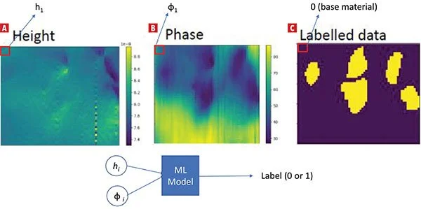
Fig. 2. Inputs are A – Height, B – Phase, and C – data with labelling (yellow- nanoparticles, purple – base material) Height and Phase data combined help identify and locate nanoparticles with C used in the training dataset (Ref. [6], Fig. 4).
What are the potential applications of machine learning in wafer characterization technologies?
With the cost of internet of things (IoT) sensors coming down, they are becoming increasingly commonplace to integrate into all areas of a cleanroom – providing real time data, data analysis, and databases integrated over the internet – collecting data and readouts from all machines used in the semiconductor wafer fabrication process. Machine Learning models can benefit from the availability of such data to be able to predict measurement and wafer characterization technologies from a broader scale as well – an ability previously unavailable. For example, if a sensor detects a change in the gas flow in a deposition process, a potential effect may be a change in the film thickness or refractive index, and this can automatically be notified to the algorithm that can consider this factor when predicting results using an ellipsometer.
Across various equipment that currently require human expert intervention and laborious trial and error processes, machine learning algorithms can help automate some of the processes involved by introducing feedback loops and referencing datasets – in a manner similar to current diagnosis and process optimization workflows. Some characterization technologies such as microscopes have advanced versions where no tuning and human intervention is required, focusing, and defocusing is automatically performed, efficiently characterizes large batches of wafer with high throughput. While the current cost of such advanced systems is quite prohibitive over time the costs would come down with improvements in algorithms – such as efficiency and accessibility. This automation could thus be integrated across other processes.
Lastly, machine learning algorithms can help predict the input parameters required for achieving a certain output characteristic, and in instances where multiple different combinations of the input parameters can help achieve the same output, based on prior data or extrapolations of functions. For example, to achieve a certain film thickness or density what are the input gas flows required in a chemical vapor deposition process. While this application is not directly related to improvements in wafer characterization technologies, a key component of this application is the accurate measurement and data collection of wafer characterizations from a wide range of processes and experimental runs. In some instances, is only a statistical problem, requiring predicting a value based on plotted functions as constraints, but a machine learning algorithm becomes useful in handling making estimations when considering larger number of inputs whose relationships may dynamically vary over time.
Conclusion
The semiconductor industry will always be driven by a need for process optimization and cost reduction, with effective and reliable wafer characterization technologies playing an essential role across the development process. Machine learning advances in terms of knowledge required, increasing availability of computation power, and increasing implementations of extensive data collection systems, data analysis algorithms, and data-driven driven decision-making have unlocked new abilities and upgrades for wafer characterization technologies. The paper explored questions such as when is a machine learning algorithm applicable, what are some limitations of wafer characterization technologies that could be potentially improved with machine learning algorithms, what are some current implementations of these algorithms and what are some other potential applications. A key parameter for effectively utilizing machine learning algorithms is the creation of large datasets with clean labelled data, however unlabeled data could also be used in certain applications. Some of the upgrades explored were defect detection through image classification of wafer maps, automatic trial-and-error feedback loops and predictions in ellipsometers, and better process control in atomic force microscopy. With the integration of larger amounts of data, they can also potentially automate other process, offer pre-emptive predictions for better batch control and throughput when inspecting wafers for defects, and estimate wafer characteristics just from considering all factors – internal and external environmental conditions – helping reduce the need for destructive measurements by enabling in-situ measurements. Machine learning algorithms hold great many applications in this field and are a step towards complete automation – achieving efficiency and cost reduction in the semiconductor chip fabrication process.
References
1. W. Lei, "Atomic Force Microscopy - Measured line width is probe shape dependent," *Metrology and Analytical Techniques*, EE6601 Advanced Wafer Processing, Feb. 27, 2024, p. 24.
2. J. C. Gallagher, M. A. Mastro, M. A. Ebrish et al., "Using machine learning with optical profilometry for GaN wafer screening," *Sci Rep*, vol. 13, p. 3352, 2023. [Online]. Available: https://doi.org/10.1038/s41598-023-29107-9
3. A. Meixner, "Fabs Drive Deeper Into Machine Learning," *Semiengineering.com*, September 7, 2021. [Online]. Available: https://semiengineering.com/fabs-drive-deeper-into-machine-learning/
4. LC. Wang and Y. Zeng, "Machine Learning Support for Wafer-Level Failure Pattern Analytics," in *Machine Learning Support for Fault Diagnosis of System-on-Chip*, P. Girard, S. Blanton, and LC. Wang, Eds. Cham: Springer, 2023, pp. 9. [Online]. Available: https://doi.org/10.1007/978-3-031-19639-3_9
5. M. Jariya, P. Kumar, R. Devi, and B. Singh, "Silicon wafer defect pattern detection using machine learning," *Materials Today: Proceedings*, vol. 2023, no. 4, p. 233, 2023. [Online]. Available: https://doi.org/10.1016/j.matpr.2023.04.233
6. I. Chakraborty and D. Yablon, "Machine learning to enhance atomic force microscopy analysis and operation," *Analyticalscience-wiley-com*, April 16, 2020. [Online]. Available: https://analyticalscience.wiley.com/content/article-do/machine-learning-enhance-atomic-force-microscopy-analysis-and-operation
Please consider supporting this article’s LinkedIn post - currently my only public social media where I share my works and hope to grow my reach.